8
THE OPERATING SYSTEM
INTRODUCTION
With every ATARI Home Computer System comes an ATARI 10K Operating System Cartridge. The importance of this cartridge is often overlooked. Without it, you have a lot of potential, but absolutely nothing else! This situation is not unique to the ATARI Home Computer System; it is encountered with all computers. A computer is, after all, merely a collection of hardware devices. A user must manage these resources to accomplish any task. If all programmers had to start from scratch on each program, we would have an even larger software shortage than we have today. The solution that has evolved over the years is to build in a program that manages the resources available to the system, and eases the programming burden required to control them. This program is known by various names: Operating System, Master Control Program, System Executive, System Monitor, etc. In the ATARI Home Computer System it is known as the Operating System or OS.
The first task facing the student of the Operating System, is to take an inventory of exactly what resources are available to the OS. These are:
- 6502 Microprocessor
- RAM Memory (various amounts)
- ANTIC LSI Integrated Circuit
- CTIA LSI Integrated Circuit
- POKEY LSI Integrated Circuit
- PIA Peripheral Interface Adapter Integrated Circuit
By using these resources, the OS can interact with and control a wide variety of external hardware devices, including a television receiver/monitor, keyboard, console speaker, console switches, joysticks, paddles, cassette recorder, disk drive, printers, RS-232 interface and modem.
The remainder of this subsection briefly lists the main elements of the OS. These elements are described in detail in following subsections.
MONITOR. The OS monitor is the system routine that is executed when the computer is turned on or the [SYSTEM RESET] button is pressed. Through this routine the OS takes control of the system; it does not relinquish control unless control is taken away from it by the programmer. The Monitor sets up the memory management system, initializes the I/O subsystem, sets up system vectors and selects the execution environment after initialization is complete.
INTERRUPT PROCESSING STRUCTURE. The computer utilizes the standard interrupt processing structure of the 6502 microprocessor, with some external augmentation for enhanced flexibility. Interrupts are generated by numerous events, including keyboard keystrokes, the [BREAK] keystroke, some serial bus events, system timer timeouts, and the vertical blank interval on the television.
OS SYSTEM VECTORS. The system vectors provide a mechanism that allows users to access system routines, or customize the OS for special needs. The most frequent uses of the vectors are to call I/O system routines, set timers, and transfer control to different execution environments. System routines may be vectored to in one of two ways. ROM vectors are locations that contain JMP instructions to system routines and cannot be altered. RAM vectors are RAM locations that contain alterable addresses of system routines. The locations of both types of vectors are guaranteed to remain the same in future releases of the OS.
INPUT/OUTPUT SUBSYSTEM. The OS gives an application programmer access to the full capabilities of the computer's peripherals. The Input/Output subsystem is a set of routines that link high level I/O operations with device handlers that control the physical I/O hardware.
REAL TIME PROGRAMMING. The ATARI Home Computer is well equipped to deal with problems in the "real time domain". To facilitate this feature, the OS has two types of timers: hardware timers and system software timers. Hardware timers are countdown timers that can be used to time events with durations that range from half a microsecond to several seconds. System timers are software timers that tick at 60 Hertz, and can be used for applications as diverse as serial bus timing and sound effect generation.
ROM CHARACTER SET. The computer is equipped with what is known as a "soft character set", i.e., It can be changed. The ROM-based character set is used to provide a standard character set at power-up.
FLOATING POINT PACKAGE. The floating point package is a set of mathematical routines that extend the arithmetic capability of the system. The routines use binary coded decimal (BCD) arithmetic to provide standard mathematical functions (+, -, *, /), exponential and logarithmic functions as well as conversion from ATASCII to BCD and BCD to ATASCII.
THE MONITOR
The OS monitor is that portion of the OS ROM that handles both the power-up and SYSTEM RESET sequences. These sequences allow the OS to gain initial control of the computer and ensure that everything is properly initialized before releasing partial control to an application program. Both sequences are similar in function and in fact share much of the same code.
The power-up routine (also known as Coldstart) is invoked either by turning on the computer or by jumping to COLDSV ($E477), a system routine vector. Important items to remember about the power-up sequence are:
- ALL of RAM memory is cleared except locations $0000-$000F.
- Both a cassette and disk boot are attempted. BOOT? ($0009) is a flag that indicates the success or failure of the boots. Bit 0 = 1 for a successful cassette boot; Bit 1 = 1 for a successful disk boot.
- COLDST ($0244) is a flag that tells the Monitor that it is in the middle of power-up. COLDST=0 means the [SYSTEM RESET] key has been pressed, whereas COLDST<>0 indicates initial power-up. The COLDST flag can be used to gain a certain amount of program security. If COLDST is set to a non-zero value during program execution, then pressing [SYSTEM RESET] will initiate the power-up sequence. This will prevent the user from gaining control of the computer while the program is running.
Pressing the [SYSTEM RESET] key causes a SYSTEM RESET (also known as Warmstart). Some of the key facts to remember about the SYSTEM RESET sequence are:
- The OS RAM vectors are downloaded from ROM during both SYSTEM RESET and power-up sequences. If you wish to "steal" a vector, some provision must be made to handle SYSTEM RESET. See the MEMORY MANAGEMENT subsection of this section for suggestions on how this is done.
- MEMLO, MEMTOP, APPMHI, RAMSIZ and RAMTOP are reset during System Reset. If you wish to alter these RAM pointers to reserve some space for assembler modules called by BASIC, you must make some provision for handling SYSTEM RESET. Figure 8-3 provides an example of how to do this.
The next few pages present a detailed flowchart for the power-up and SYSTEM RESET sequences.
Figure 8-1.1 System Initialization
Figure 8-1.2 System Initialization
Figure 8-1.3 System Initialization
Figure 8-1.4 System Initialization
MEMORY MANAGEMENT
The fact that the OS is written for a 6502 microprocessor dictates a number of overall memory management decisions. In the 6502, there are three special regions in the memory address space. Page zero has crucial significance in that the use of data values on this page will result in tighter, faster executing code. Indeed, there are instructions that absolutely require page zero locations to work. Page one is special because it is used for the 6502 stack. Addresses $FFFA - $FFFF are also special because they are reserved for hardware reset and interrupt vectors.
Thus, the first task of memory management is to assign the OS ROM to the highest part of memory address space. The OS resides in the address space from $D800 to $FFFF. Just under this area is the space reserved for the hardware registers in ANTIC, CTIA, and POKEY. These reside in the $D000-$DFFF range.
At the other end of memory address space, the OS reserves half of page zero for its own use. Pages two, three, four and five are also reserved for OS usage. From a programming viewpoint, the usable memory area runs from $0600 to $BFFF.
When the system is powered-up, one of the first actions taken by the OS is to determine how much RAM memory is present. This is accomplished by checking the first byte of each 4K block of memory starting at $1000. The contents of this byte are read, complemented and an attempt is made to store the complemented value back out. If this attempt is successful, the temporary memory size counter is incremented by 4K. This process continues until a location is found that cannot be changed. Two variables, RAMTOP and RAMSIZ contain the number of RAM pages present. In addition to these locations, pointers MEMLO, MEMTOP, and APPMHI are maintained by the OS memory management routines. The relationships between these pointers are shown in Figure 8-2, a simple memory map.
MEMLO is a 2-byte location that the OS uses to indicate where an application program may begin. You can modify MEMLO to create reserved areas for assembly language routines that may be called from BASIC. BASIC uses the value in MEMLO to determine the starting location of a program (see Section 10 for a discussion of the structure of a BASIC program). If the value of MEMLO is changed to a higher address, it must be done before control is transferred to the BASIC cartridge. This is a tricky operation, because MEMLO is reset by both power-up and SYSTEM RESET.
If an application program is running in a disk drive environment, the AUTORUN.SYS facility can be used to change MEMLO to reserve space. However, DOS is also initialized during SYSTEM RESET via the DOSINI vector ($000C). This vector contains the address of the DOS initialization code called as part of the monitor system initialization. DOSINI is also the only point at which you can "trap" the SYSTEM RESET sequence. Since the DOS initialization must occur regardless of what is done to the MEMLO pointer, you must allow the normal initialization to occur before "stealing" the DOSINI vector. This may be done by moving the contents of DOSINI into the 2-byte address of a JSR information on the AUTORUN.SYS feature). Just after the JSR instruction, place the code which sets MEMLO to a new value. Follow this with a RTS instruction. DOSINI must then be reset to the address of the JSR instruction. When a SYSTEM RESET occurs, the new code sequence is called and the first instruction, JSR OLDDOSINI, initializes DOS. The remaining code is then executed which sets MEMLO to its new value and then rejoins the rest of the initialization sequence. Figure 8-3 presents an example showing how to do this.
The above technique can also be used with MEMTOP, the user high memory pointer. This pointer indicates the highest RAM address accessible to an application program. This RAM address differs from the highest physical RAM address because the OS allocates some RAM at the very top of RAM for its display list and display data. Space for assembly language modules and data can be set aside by lowering MEMTOP from the values set by power-up and SYSTEM RESET. Using MEMTOP instead of MEMLO to reserve space does create one problem. The value of MEMTOP depends on both the amount of RAM in the system and the graphics mode of the display. This makes it difficult to predict its value before actually examining the location unless you make assumptions about the system configuration. This uncertainty over the final location of the machine code forces the programmer to use only relocatable code.
APPMHI is a location that contains an address specifying the lowest address to which the display RAM may extend. Correctly setting APPMHI ensures that the display handler will not clobber some of your program code or data.
RAMSIZ, like MEMTOP, can also be used to reserve space for user routines or data. Since RAMSIZ is a single byte value that contains the number of RAM pages present (i.e., groups of 256 bytes), lowering its value by 1 will reserve 256 locations. The advantage of using RAMSIZ instead of MEMTOP is that the space saved by moving RAMSIZ down is above the display memory, whereas space saved by moving MEMTOP down remains below the display memory.
Figure 8-2 OS and BASIC Pointers (DOS present)
            0010 ; RESET THE MEMLO POINTER
            0020 ;
0600        0030 START    =    $600
000C        0040 DOSINI   =    $0C
02E7        0050 MEMLO    =    $2E7
3000        0060 NEWMEM   =    $3000     ; THIS IS THE NEW VALUE FOR MEMLO
            0065 ;
            0070 ; THIS ROUTINE RESERVES SPACE FOR ASSEMBLY ROUTINES
            0090 ; BY RESETING THE MEMLO POINTER. IT RUNS AS
            0100 ; AN AUTORUN.SYS FILE. IT ALSO RESETS MEMLO ON [RESET].
            0120 ; MEMLO IS SET TO THE VALUE OF NEWMEM.
            0130 ;
            0140 ; THIS PART IS PERMANENT, IE. NEEDS TO BE RESIDENT.
            0150 ; THE SYSTEM DOSINI VECTOR HAS BEEN STOLEN
            0160 ; AND STORED IN THE ADDRESS PORTION OF THE JSR TROJAN
            0170 ; INSTRUCTION. SO WHEN [RESET] IS PRESSED, DOSINI VECTORS
            0180 ; TO INITDOS, JSR TROJAN THEN CALLS THE DOS INITIALIZATION
            0185 ; ROUTINES, MEMLO IS RESET TO NEW VALUE AND CONTROL
            0190 ; RETURNS TO THE MONITOR.
0000        0200        *=       START
            0210 INITDOS
0600 200D06 0220        JSR  TROJAN   ; DO DOS INITIALIZATION
0603 A900   0230        LDA  #NEWMEM&255
0605 8DE702 0240        STA  MEMLO
0608 A930   0250        LDA  #NEWMEM/256
060A 8DE802 0260        STA  MEMLO+L
            0270 TROJAN
060D 60     0280        RTS
            0290 ; THIS PART IS EXECUTED AT POWER UP ONLY AND
            0300 ; CAN BE DELETED AFTER POWER-UP.
            0330 ; THIS ROUTINE STORES THE CONTENTS OF DOSINI INTO THE JSR
            0350 ; TROJAN INSTRUCTION. IT THEN REPLACES DOSINI WITH
            0370 ; A NEW VALUE, LOCATION INITDOS.
            0390 GRABDOSI
060E A50C   0400        LDA  DOSINI        ; SAVE DOSINI
0610 8D0106 0410        STA  INITDOS+1
0613 A50D   0420        LDA  DOSINI+1
0615 8D0206 0430        STA  INITDOS+2
0618 A900   0440        LDA  #INITDOS&255  ; SET DOSINI
061A 850C   0450        STA  DOSINI
061C A906   0460        LDA  #INITDOS/256
061E 850D   0470        STA  DOSINI+1
0620 A500   0480        LDA  NEWMEM&255    ; SET MEMLO
0622 8DE702 0490        STA  MEMLO
0625 A930   0500        LDA  #NEWMEM/256
0627 8DES02 0510        STA  MEMLO+1
062A 60     0520        RTS
062B        0530        *=   $2E2
02E2 0E06   0540        .WORD GRABDOSI     ; SET RUN ADDRESS
02E4        0550        .END
Download / View CH8PRG1.SRC (Listed ASSEMBLY)
Figure 8-3 Reset MEMLO
INTERRUPT PROCESSING STRUCTURE
The capability to selectively respond to special hardware and software events (i.e. interrupts), provides enormous flexibility to any computer system. As in any 6502-based system, there are two types of interrupt requests at the processor level, maskable (IRQ) and nonmaskable (NMI) interrupts. A higher level of interrupt control is provided by ANTIC, POKEY and the PIA chip. Each of these chips is responsible for mediating a number of events which could cause interrupts. If a particular interrupt is enabled at the level of the three guardian chips, then they allow the interrupt request to pass on to the 6502. ANTIC handles NMI requests, and POKEY and the PIA handle IRQ requests.
The following interrupt functions are available:
| Name (vector) | Type | Function | Used By |
|---|---|---|---|
| DISPLAY LIST (VDSLST) SYSTEM RESET (none) VERTICAL BLANK (VVBLKI,VVBLKD) SERIAL INPUT READY (VSERIN) SERIAL OUTPUT READY (VSEROR) SERIAL OUTPUT COMPLETE (VSEROC) POKEY TIMER 1 (VTIMR1) POKEY TIMER 2 (VTIMR2) *POKEY TIMER 4 (VTIMR4) KEYBOARD (VKEYBD) *BREAK KEY (BRKKY) SERIAL BUS PROCEED (VPRCED) SERIAL BUS INTERRUPT (VINTER) |
NMI NMI NMI IRQ IRQ IRQ IRQ IRQ IRQ IRQ IRQ IRQ IRQ |
Graphics timing System init. Graphics display Serial input Serial output Serial output Hardware timer Hardware timer Hardware timer Key pressed [BREAK] key Device proceed Device interrupt |
User OS OS,user OS OS OS User User User OS OS Unused Unused |
* This IRQ is vectored only in the Rev. B version of the OS
Section 6 of the OPERATING SYSTEM Manual contains more detailed information on interrupts. Extreme care needs to be taken in working with interrupts. For example, if you accidentally disable the keyboard IRQ interrupt, the computer will ignore all the keys except the [BREAK] key. Although this may be useful sometimes, it may make debugging your program a bit difficult!
The IRQ Interrupt Handler
The OS has an IRQ interrupt handler that processes the various IRQs. This handler has RAM vectors for all of the IRQs. (Note – the [BREAK] key IRQ is not vectored in the original version of the OS The IRQ vectors are set to their initial values during both power-up and SYSTEM RESET. The locations of the IRQ RAM vectors are described in the subsection on System Vectors.
IRQ vector functions are:
VIMIRQ - Immediate IRQ vector. All IRQs vector through this location. VIMIRQ normally points to the system IRQ handler. You can steal this vector to do your own IRQ Interrupt processing.
VSEROR - Pokey Serial Output Needed IRQ vector. This normally points to the code to provide the next byte in a buffer to the serial output port.
VSERIN - Pokey Serial Input Ready IRQ vector. This points to the code to place a byte from the serial input port into a buffer.
VSEROC - Pokey Serial Output Complete IRQ vector. Normally this vector points to code that sets a transmit done flag after the checksum byte goes out.
VTIMR1 - Pokey Timer 1 IRQ vector. Initialized to point to a PLA,RTI instruction sequence.
VTIMR2 - Pokey Timer 2 IRQ vector. Initialized to point to a PLA,RTI instruction sequence.
VTIMR4 - Pokey Timer 4 IRQ vector. Initialized to point to a PLA,RTI instruction sequence.
VKEYBD - Keyboard IRQ vector. Pressing any key except [BREAK] causes this IRQ. VKEYBD can be used to preprocess the key code before it is converted to ATASCII by the OS. VKEYBD normally points to the OS keyboard IRQ routine.
BRKKY - [BREAK] key vector. In the Rev. B version of the OS, this IRQ has its own vector. It is initialized to a PLA,RTI instruction sequence.
VPRCED - Peripheral Proceed IRQ vector. The proceed line is available to peripherals on the serial bus. This IRQ is unused at present and normally points to a PLA,RTI instruction sequence.
VINTER - Peripheral interrupt IRQ vector. The interrupt line is also available on the serial bus. VINTER normally points to a PLA,RTI instruction sequence.
VBREAK - 6502 BRK instruction IRQ vector. Whenever a software break instruction is executed, this interrupt occurs. VBREAK can be used to set break points for a debugger, though it normally points to a PLA,RTI instruction sequence.
The IRQs are enabled and disabled as a group by the 6502 instructions CLI and SEI respectively. The IRQs also have individual enable/disable bits in POKEY. The programmer's reference card provided with this book shows the IRQs and their enable/disable bits.
The IRQEN register contains most of the IRQ enable/disable bits and is a write-only register. The OS keeps a shadow copy of IRQEN in POKMSK ($0010), but IRQEN is not updated from POKMSK during vertical blank. Each interrupt is enabled by setting the proper bit in IRQEN to a one. A zero is placed in a bit in IRQEN to clear interrupt status from that corresponding bit in IRQST. You might note that bit 3 in IRQST (Serial data transmission is finished) is not cleared by this process. This bit is simply a status bit and reflects the current status of the serial transmission register.
PACTL and PBCTL are used to enable and test the status of the IRQs handled by the PIA. Bit 0 of each of these registers is the interrupt enable for that port. Bit 7 represents the interrupt status. This bit is cleared whenever the PACTL or PBCTL registers are read.
Using The IRQs
The availability of the IRQ vectors means that you can tailor much of the system I/O to your liking. Currently, the OS does not provide for overlapping I/O with other processing. By redirecting the three serial I/O interrupt vectors however, it is possible to rewrite portions of the I/O subsystem to allow for true concurrent processing.
The three timer interrupts can be put to use in any operation requiring precise timing control. These timers would normally be used when the 60-Hertz software timers are too slow. Refer to the subsection on Real Time Programming for more information on this topic.
Many applications require that programs be protected from user input error. A couple of the IRQ vectors can be used to provide extended input protection. The example in Figure 8-4 uses the VKEYBD IRQ vector to disable the control key. The routine also masks the [BREAK] key by stealing the VIMIRQ vector and ignoring the [BREAK] key interrupt. Though written for the original version of the OS, this routine will still work in Rev. B.
Two of the IRQs are handled by the PIA, VPRCED and VINTER. These are unused by the OS, and may be utilized to provide more control over external devices.
0010        10 POKMSK   =    $0010
D209        20 KBCODE   =    $D209
0208        30 VKEYBD   =    $0208
D20E        40 IRQEN    =    $D20E
D20E        45 IRQST    =    IRQEN
0216        46 VMIRQ    =    $0216
0000        60          *=   $600
0600 78     80 START    SEI                 DISABLE IRQS
0601 AD1602 90          LDA     VMIRQ       REPLACE THE IRQ VECTOR
0604 8D4D06 0100        STA     NBRK+1      WITH OUR OWN
0607 AD1702 0110        LDA     VMIRQ+1     ALL IRQS WILL
060A 8D4E06 0120        STA     NBRK+2      GO TO NBRK
060D A945   0130        LDA     #IRQ&255
060F 8D1602 0140        STA     VMIRQ
0612 A906   0150        LDA     #IRQ/256
0614 8D1702 0160        STA     VMIRQ+1
0617 AD0802 0200        LDA     VKEYBD      POINT KEY IRQ TO
061B 8D4306 0210        STA     JUMP+1      REP
061E AD0902 0220        LDA     VKEYBD+1
0621 8D4406 0230        STA     JUMP+2
0624 A939   0240        LDA     #REP&255    VECTOR KEY IRQ
0626 8D0802 0250        STA     VKEYBD      LOW BYTE OF VECTOR
0629 A906   0260        LDA     #REP/256
062B 8D0902 0270        STA     VKEYBD+1
062E 58     0170        CLI                 ENABLE IRQS
062F 60     0280        RTS
            0290        *=$639
0639 AD09D2 0300 REP    LDA     KBCODE      ALL KEY IRQS COME HERE
063C 2980   0310        AND     #$80        CHECK IF CONTROL HIT
063E F002   0320        BEQ     JUMP        IF NOT HIT THEN GO
0640 68     0330        PLA                 ELSE IGNORE CONTROL KEY
0641 40     0340        RTI
0642 4C4206 0360 JUMP   JMP     JUMP        THIS CALLS THE OLD KEY IRQ
0645 48     0375 IRQ    PHA                 ALL IRQS COME HERE
0646 AD0ED2 0380        LDA     IRQST       CHECK IF [BREAK]
0649 1004   0390        BPL     BREAK       IF [BREAK] IRQ,BRANCH
064B 68     0405        PLA                 ELSE CALL OLD IRQ VECTOR
064C 4C4C06 0410 NBRK   JMP     NBRK        CALL OLD IRQ VECTOR
064F A97F   0430 BREAK  LDA     #$7F        HERE IF [BREAK]
0651 8D0ED2 0440        STA     IRQST       SHOW NO [BREAK]
0654 A510   0450        LDA     POKMSK
0656 8D0ED2 0460        STA     IRQEN
0659 68     0462        PLA
065A 40     0464        RTI                 RETURN AS IF NO [BREAK]
065B        0470        *=   $02E2
02E2 0006   0480        .WORD START
Download / View CH8PRG2.SRC (Listed ASSEMBLY)
Figure 8-4 Protecting Programs from User Input Error
The NMI Handler
The OS has an NMI handler for handling the nonmaskable interrupts. Unlike the IRQs, the NMIs cannot be "masked" (disabled) at the 6502 level. All the NMIs except SYSTEM RESET can be disabled by ANTIC.
Two of the NMIs, the display list interrupt (DLI) and the vertical blank (VBLANK) interrupt, have RAM vectors that can be used. In fact, VBLANK can be intercepted in two places, immediate or deferred VBLANK. The NMI vectors are:
| Name | Vector |
|---|---|
| SYSTEM RESET DISPLAY LIST INTERRUPT VERTICAL BLANK IMMEDIATE DEFERRED |
none VDSLST ($0200) VVBLKI ($0222) VVBLKD ($0224) |
The SYSTEM RESET NMI doesn't have a RAM vector. SYSTEM RESET always results in a jump to the monitor warmstart routine. However, the DOSINI RAM vector is used during the Warmstart process, and thus can be used to trap the [SYSTEM RESET] (see subsection on the Monitor).
The DLI vector is unused by the OS. Refer to Section 5, Display List Interrupts, for details on using this feature.
Vertical Blank Interrupt Processing
The vertical blank interrupt facility is an extremely valuable resource to a programmer. These interrupts are nonmaskable and occur at regular intervals based on the television signal standard (every 60th of a second for NTSC, every 50th for PAL). Just as importantly, these interrupts occur during that period of time when the screen has been blanked, so that changes made during this period will not be immediately seen on the display. This leads to a wide assortment of uses.
After a vertical blank interrupt has been recognized by the OS, the contents of the A, X, and Y registers are placed onto the stack. The system then vectors through the immediate vertical blank vector (VVBLKI) located at $0222. This vector normally points to the OS vertical blank interrupt service routine at $E45F. The OS uses this routine to increment the real time clock, to decrement the system timers, to do color attracting, to copy shadow registers,. and to update values from the input controllers. This routine terminates by jumping through the deferred vertical blank vector (VVBLKD) at $0224. This vector is initialized to point to a simple interrupt termination routine at $E462. Figure 8-5 illustrates this process.
Figure 8-5 Vertical Blank Interrupt Execution
These two vectors were put into RAM to allow programmers to trap the vertical blank service routine and use the 60-Hertz interrupt for their own purposes. The procedure to use them is straightforward. First decide whether the vertical blank interrupt (VBI) routine is to be an immediate VBI or a deferred VBI. In many cases it makes little difference which is chosen. There are some instances where it does matter. The first case arises when your VBI routine reads or writes to registers which are shadowed by the OS VBI routine. It might be necessary to write to the hardware registers after the OS VBI has written to them. He who writes last, writes best!
The second case arises when your VBI routine consumes too much processor time. The OS VBI routine may then be delayed beyond the end of the vertical blank period. This in turn may cause some graphics registers to be changed while the beam is tracing on the screen. The result may be unsightly. if this is the case, your VBI routine should be placed as a deferred VBI routine. The time limit for immediate VBI is about 2000 machine cycles; for deferred VBI it is about 20,000 cycles. However, many of these 20,000 machine cycles are executed while the electron beam is being drawn, so graphics operations should not be executed in extremely long deferred VBI routines. Furthermore, display list interrupt execution time comes out of the time available for this processing. Remember, VBI processing will cut down on the time available for mainline code execution.
The third case arises when your own VBI must be mixed with time-critical I/O such as to the disk or cassette. The OS immediate VBI routine has two stages, a critical and a non-critical stage. During time critical I/O, the OS immediate VBI routine aborts after stage one processing is complete. if you want your VBI to be executed during every vertical blank period, it must be defined as an immediate VBI. Be wary in this situation, for this may result in interference problems with time-critical I/O.
Once you have decided whether your VBI routine should be immediate or deferred, you must place the routine in memory (page six is a good place), link it to the proper VBI routine, and modify the appropriate OS RAM vector to point to it. Terminate an immediate VBI routine with a JMP to $E45F. Terminate a deferred VBI routine with a JMP to $E462. If you want to bypass the OS VBI routine entirely (and thereby gain processing time), terminate your immediate VBI routine with a JMP to $E462.
A common problem with interrupts on 8-bit micros arises when you try to change the vector to the interrupt. Vectors are 2-byte quantities; it takes two store instructions to change them. There is a small chance that an interrupt will occur after the first byte has been changed but before the second byte has been updated. This could crash the system. The solution to this problem has been provided by an OS routine called SETVBV at $E45C. Load the 6502 Y-register with the low byte of the address, the X-register with the high byte of the address, and the accumulator with a 6 for immediate VBI or a 7 for deferred VBI. Then JSR SETVBV and the interrupt will be safely enabled. The new VBI routine will begin executing within one 60th of a second.
A wide variety of operations can be performed with 60-Hertz interrupts. First, screen manipulations can be done during the vertical blank to ensure that transitions do not occur on the screen. Second, high speed regular screen manipulations can be performed. This can be very important in rhythmic animations where changes need to occur at a pace independent from other processing.
Another function of vertical blank interrupts is for real-time sound effects. The sound registers in the ATARI 400/800 allow control of frequency, volume, and distortion, but not duration. Duration can be controlled with a VBI by having a calling routine set some duration parameter which the VBI then decrements down to zero. This technique can be used to control the volume of the sound and so give attack and decay envelopes to sounds. Finer control of frequency and distortion is possible with extensions of this technique. The result can be very intricate sound effects. Since the VBI time resolution is only 1/60th of a second, VBls are not useful for the volume only mode of the audio channels.
VBls are also useful for handling user inputs. Usually, these inputs require little processing, but constant attention. A VBI allows the program to check for user input every 60th of a second without burdening the' program. It is an ideal solution to the problem of maintaining computational continuity without ignoring the user.
Finally, VBls allow a crude form of multitasking to take place. A foreground program can run under the VBI while a background program runs in the mainline code. As with any interrupt, careful separation of the databases for the two programs must be maintained. The power derived from the vertical blank interrupt is, however, well worth the effort.
THE SYSTEM VECTORS
One measure of the power of any operating system is its adaptability. Just how easy is it for a user to take advantage of the OS routines or modify and customize system routines?
In this regard, the OS for the ATARI Home Computer System would score well. In practically every instance where access to system routines could be beneficial, the OS has "hooks" where you can attach or replace system routines with your own.
This flexibility is provided by a combination of several different mechanisms. The first of these is a ROM table of JMP instructions to crucial OS routines. In future versions of the OS, the location of this Jump table will not change, although the values there probably will. Thus, if your software accesses the main OS routines via this table, it will also work on future versions of the OS. If your software does not use these ROM vectors, but instead jumps directly into the OS ROM, then it will almost certainly crash on future versions of the OS.
The second mechanism is a series of address vectors in RAM which link many of the interrupt processing routines together. To alter the handling of a particular interrupt, one need change only a single vector to point to the replacement code. The OS initializes these vectors as part of the power-up sequence. Again, though the initialized contents of these vectors may change, their location is guaranteed not to.
The third mechanism is the device handler table where vectors to specific device handlers (e.g. disk drive, printer,...) are stored. For a discussion of this facility, refer to the Centralized Input/Output subsection of this section.
| Name | Location | Use |
|---|---|---|
| DISKIV DSKINV CIOV SIOV SETVBV SYSVBV XITVBV SIOINV SENDEV INTINV CIOINV BLKBDV WARMSV COLDSV RBLOKV CSOPIV |
$E450 $E453 $E456 $E459 $E45C $E45F $E462 $E465 $E468 $E46B $E46E $E471 $E474 $E477 $E47A $E47D |
Disk handler initialization Disk handler vector Central I/O routine vector Serial I/O routine vector Set system timers routine vector System vertical blank processing Exit vertical blank processing Serial I/O initialization Serial bus send enable routine Interrupt handler routine Central I/O initialization Blackboard mode (Memopad) vector Warm start entry point (SYSTEM RESET) Cold start entry point (power-up) Cassette read block routine vector Cassette open for input vector |
Figure 8-6 ROM Jump Vectors
Since this ROM table is actually a table of three byte JUMP instructions, an example of using a ROM vector is:
JSR CIOV
RAM VECTORS
| Name | Location | Value | Use |
|---|---|---|---|
| -- Page Two Locations -- | |||
| VDSLST VPRCED VINTER VBREAK VKEYBD VSERIN VSEROR VSEROC VTIMR1 VTIMR2 VTIMR4 VIMIRQ VVBLKI VVBLKD CDTMA1 CDTMA2 BRKKY |
$0200 $0202 $0204 $0206 $0208 $020A $020C $020E $0210 $0212 $0214 $0216 $0222 $0224 $0226 $0228 $0236 |
$E7B3 $E7B3 $E7B3 $E7B3 $FFBE $EB11 $EA90 $EAD1 $E7B3 $E7B3 $E7B3 $E6F6 $E7D1 $E93E $xxxx $xxxx $E754 |
Display List Interrupt NMI Vector Proceed Line IRQ Vector -- Unused at present Interrupt Line IRQ Vector -- Unused at Present Software Break Instruction IRQ Vector Keyboard IRQ Vector Serial Input Ready IRQ Vector Serial Output Ready IRQ Vector Serial Output Complete IRQ Vector POKEY Timer 1 IRQ Vector POKEY Timer 2 IRQ Vector POKEY Timer 4 IRQ Vector Vector to IRQ Handler Immediate Vertical Blank NMI Vector Deferred Vertical Blank Vector System Timer 1 JSR Address System Timer 2 JSR Address BREAK key Vector (** only Rev. B **) |
| -- Page Zero Locations -- | |||
| CASINI DOSINI DOSVEC RUNVEC INIVEC |
$0002 $000C $000A $02E0 $02E2 |
$xxxx $xxxx $xxxx $xxxx $xxxx |
Vector for bootable cassette program initialization Disk Initialization Vector Disk Software Run Vector DUP File Load and GO Run Vector DUP File Load and Go Initialization Vector |
An x Indicates that the contents of this location may vary
Figure 8-7 RAM Vectors
Unlike the ROM Jump tables, these vectors are true two byte address vectors. A typical calling sequence to use one of the RAM vectors might look like this:
      JSR CALL
CALL  JMP (DOSINI)
THE CENTRALIZED INPUT/OUTPUT SUBSYSTEM
One of the most taxing problems facing an operating system designer is how to handle input/output to the wide variety of peripherals that might be hooked up to the system. A few general philosophical guidelines to efficient I/O handling are:
- The transfer of data should be device-Independent.
- The I/O structure should support single-byte, multiple-byte, and record-organized data transfers.
- Multiple devices/files should be concurrently accessible.
- Error handling should be device-transparent.
- The addition of new device handlers should be possible without having to change the OS ROM.
The ATARI 400/800 OPERATING SYSTEM (OS) was designed to provide exactly these capabilities. The ATARI 400/800 OS uses a table-driven centralized input/output subsystem. From the OS standpoint, I/O is organized around the IOCB, or Input/Output Control Block. An IOCB is a standard table that specifies one complete input or output operation. Any of eight standard I/O operations can be executed through an IOCB. By changing an entry in the IOCB, the user can change the nature of the input/output operation, even the physical device which is the target of the I/O. Thus, a user can easily perform I/O to completely different devices such as the disk drive and the printer without having to worry about hardware details. Most I/O requires only that the user set up an IOCB with control data, and then pass control to the I/O subsystem.
Two types of elements make up the I/O subsystem: I/O system routines and I/O system control blocks. The I/O system routines include the central I/O routine (CIO), the device handlers (E:, K:, S:, P:, C:, D:, R:) and the serial I/O routine (SIO). The Handler Address Table (HATABS) plays a major role in linking CIO with the individual device handlers. The system I/O control blocks contain control data that is routed to the I/O subsystem. The user interface is the same for all devices (e.g., the commands to output a line to the printer (P:) or to the display editor (E:) are very similar).
Understanding the structure of the I/O subsystem will enhance your use of it. Figure 8-8 shows the relationship of the I/O system routines and the I/O system control blocks.
Figure 8-8 I/O Subsystem
I/O System Control Blocks
There are four types of control blocks:
-Input/Output Control Block (IOCB)
-Zero-Page I/O Control Block
(ZIOCB)
-Device Control Block (DCB)
-Command Frame Buffer (CFB)
The I/O system control blocks are used to communicate information about the I/O function to be executed. The control blocks provide the I/O system routines with control information to perform the I/O function. Refer to the OPERATING SYSTEM Manual for information as to the detailed structure of the four types of control blocks.
Eight IOCBs in the OS are used to effect communication between user programs and CIO. Figure 8-9 shows the content of an IOCB for some common I/O functions. The IOCBs are:
| Name | Location, Length |
|---|---|
| IOCB0 IOCB1 IOCB2 IOCB3 IOCB4 IOCB5 IOCB6 IOCB7 |
[$340,16] [$350,16] [$360,16] [$370,16] [$380,16] [$390,16] [$3A0,16] [$3B0,16] |
A second type of control block, the ZIOCB [$0020,16], is used to communicate I/O control data between CIO and the device handlers. When called, CIO uses the value contained in the X-register as an index to which of the IOCBs (one of eight) is to be used. CIO then moves the control data from the selected IOCB to the ZIOCB for use by the appropriate device handler. The ZIOCB is of little interest unless you are writing a new device handler or are replacing a current one.
Device handlers that require I/O over the serial bus will then load control information into the DCB [$0300,12]. SIO will use the DCB information and return the status information in the DCB for subsequent use by the device handler. Figure 8-10 illustrates some common I/O functions and the contents of their associated DCBs.
The resident disk handler does not conform to the regular user-CIO-handler-SIO calling sequence. Instead, you use the DCB to communicate directly with the resident disk handler. Section 9, the Disk Operating System, contains more information on the resident disk handler.
The last type of control block encountered in the I/O subsystem is the Command Frame Buffer (CFB). This 4-byte table located at $023A is used by the SIO routine while performing the serial bus operations. The four bytes contain the device code, command code, and command auxiliary bytes 1 and 2. The data buffer that is transmitted is defined by two pointers BUFRLO [$0032,2] and BFENLO [$0034,2]. In general it is not recommended that the OS be used at this level. Other parameters have to be set, and extreme care must be taken in calling the proper sequence of subroutines. CIO and SIO were designed to be easily called by user programs. Use them — but stay away from the command frame buffer!
IOCB CHART
| CALL | ICHID | ICDNO | ICCOM | ICSTA | ICBAL | ICBAH | ICPTL | ICPTH | ICBLL | ICBLH | ICAX1 | ICAX2 |
|---|---|---|---|---|---|---|---|---|---|---|---|---|
| OPEN FILE-READ OPEN FILE-WRITE GET BYTES PUT BYTES GET RECORD PUT RECORD CLOSE FILE STATUS |
X X X X X X X X |
X X X X X X X X |
3 3 7 $B 5 9 $C $D |
note 1 note 1 note 1 note 1 note 1 note 1 note 1 note 1 |
$80 $80 00 00 00 00 X X |
06 06 06 06 06 06 X X |
X X X X X X X X |
X X X X X X X X |
X X $80 $80 $80 $80 X X |
X X 00 00 00 00 X X |
4 8 X X X X X X |
0 note 2 X X X X X X |
|
Note 1=The status of the I/O command is stored here and in the Y REG. on return from CIO. Note 2=The Auxilary bytes of the IOCB's are used by some handlers to indicate special modes. X = Indicates ignore but do not change the current value. GENERAL NOTE: The above IOCB definitions assume: *=$600
|
Figure 8-9 Input Output Control Block (IOCB)
DCB CHART
| FUNCTION | NAME | LOCATION | DISK 810/815 | PRINTER 820 WRITE | |||||
|---|---|---|---|---|---|---|---|---|---|
| READ SECTOR | WRITE SECTOR | PUT | FORMAT | ||||||
| 810 | 815 | 810 | 815 | ||||||
| Serial Bus I.D. Device Number Command Byte Status Buffer Address Device Timeout Buffer Length |
DDEVIC DUNIT DCOMND DSTATS DBUFLO DBUFHI DTIMLO DBYTLO DBYTHI DAUX1 DAUX2 |
[$0300] [$0301] [$0302] [$0303] [$0304] [$0305] [$0306] [$0308] [$0309] [$030A] [$030B] |
$30 1-4 $52 $40 U U $30 $80 $00 2* 2* |
$30 1-8 $52 $40 U U $30 00 01 2* 2* |
$30 1-4 $57 $80 U U $30 $80 $00 2* 2* |
$30 1-8 $57 $80 U U $30 00 01 2* 2* |
$30 1-4 $50 $80 U U $31 $80/00 $00/01 - 2* - 2* |
$30 1-4 $21 $40 U U $130 - - - - |
$30 1 $57 $80 U U 5 $40 $00 1* 1* |
|
1* = This bytes determines printer mode (see 820 manual). 2* = DAUX1 + DAUX2 specify sector for READ, WRITE (PUT), or WRITE verify. U = Indicates user-set address - = Indicates ignored |
Figure 8-10 Device Control Block (DCB)
Central I/O System Routine
The main function of CIO is to take control data from an IOCB and ensure that it is routed to the specific device handler needed, and then to pass control to that handler. CIO also acts as a pipeline for most I/O in the system. Most of the OS I/O functions use CIO as a common entry point, and all handlers exit via CIO. For example, BASIC will call CIO when performing an OPEN or a GRAPHICS statement. CIO supports the following functions:
| OPEN CLOSE GET CHARS READ RECORD PUT CHARS WRITE RECORD STATUS SPECIAL |
Device/file open Device/file close Read N characters Read next record Write N characters Write next record Get device status Device handler specific (e.g., NOTE for FMS) |
You may wish to make your own CIO calls. The calling sequence for CIO is:
                       ;rem user has already set up IOCB
        LDX #IOCBNUM   ;set the IOCB index (IOCB * 16)
        JSR CIOV       ;system routine vector to CIO
        BMI ERROR      ;if branch taken then CIO returned
                       ;error code in Y-register
As shown in the above call, one of the IOCBs is used to communicate control data to CIO. You may use any one of the eight IOCBS. CIO expects the IOCB index to be in the X-register. Note that this value must be the IOCB number multiplied by 16. The reason is that CIO uses this value as a true index into the various IOCBs, and each IOCB is 16 bytes. Upon return, the sign bit of the 6502 is set to indicate success or error in the I/O operation. If the N-bit is clear (i.e., a zero) the I/O was done successfully, and the Y-register will contain a 1. If the N-bit is set, the I/O request resulted in an error; in that case the Y-register will contain the error code number. A BMI instruction to an error routine is the usual way to test for operational success. The error/success value is also returned in the IOCB byte ICSTA (see IOCB definition). Chapter 5 of the OPERATING SYSTEM Manual has a sample program segment that calls CIO to OPEN a disk file, READ some records., then CLOSE the file.
CIO copies the control data from the selected IOCB to the page zero ZIOCB. CIO then determines the device handler entry point and vectors to the appropriate device handler routine. Figure 8-11 is a flowchart of the CIO system routine.
Figure 8-11.1 CIO Routine
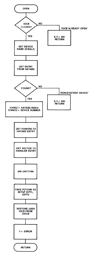
Figure 8-11.2 CIO Routine
The Handler Address Table
CIO calculates the device handler entry point in an indirect manner. First of all, an OPEN call must preceed any other I/O function to a device. While processing an OPEN command, CIO retrieves the device specification for the file being opened. The device specification is an ATASCII string pointed to by the buffer address portion of the IOCB. The first element in this string must be a one character device identifier (e.g., 'D' for disk drive, 'P' for printer,...). CIO then searches for this character in a table of handler entry points called HATABS, which runs from $031A to $033B (Figure 8-12 shows the layout of HATABS). CIO begins the search at the bottom of HATABS and works upward until a match is found for the device identifier. The search is performed in this direction to facilitate the addition or modification of device handlers. During the initialization code, the HATABS table is copied from ROM down into RAM. Devices that are then booted (e.g. the disk drive, or RS-232 module) then add their handler information to the bottom of the table. There is room in the table for a total of 14 entries, 5 of which are set up during system initialization. If a new printer handler were added to the bottom of the table, CIO would find it before the one transferred from ROM. This allows new handlers to replace old ones.
After the device identifier has been located, CIO knows that the next two bytes point to the devices' entry point table. This is a table of addresses for the routines that handle each of the CIO functions. Figure 8-13 gives the layout of a typical entry point table.
To find which one of the handler entry points to vector through, CIO then uses ICCOM, the IOCB command byte, as an index into the entry table. The entry point tables for all of the resident device handlers can be found in the OS listing. The relative position of each of the vectors in an entry table have the same meaning from table to table. For example, the first position in all of the device handler entry point tables is the vector to the device handler OPEN routine.
You can take advantage of the flexibility of HATABS to add some new features to the OS. Figure 8-14 is an example of how to add a null handler. A null handler does exactly what its name implies: nothing. This can be useful in debugging programs. Instead of waiting around for 50,000 disk accesses to find a bug, output can be directed to the null handler. With a null handler, trouble spots in programs can be identified more quickly.
            01 ; HANDLER ADDRESS TABLE
E430        02 PRINTV  =     $E430
E440        03 CASETV  =     $E440
E400        04 EDITRV  =     $E400
E410        05 SCRENV  =     $E410
E420        06 KEYBDV  =     $E420
            07 ;
0000        08         *=   $031A
            09 ;
            10 HATABS
031A 50     20         .BYTE   'P'     PRINTER
031B 30E4   30         .WORD    PRINTV    ENTRY POINT TABLE
031D 43     40         .BYTE   'C'     CASSETTE
031E 40E4   50         .WORD   CASETV     ENTRY POINT TABLE
0320 45     60         .BYTE   'E'     DISPLAY EDITOR
0321 00E4   70         .WORD   EDITRV     ENTRY POINT TABLE
0323 53     80         .BYTE   'S'     SCREEN HANDLER
0324 10E4   90         .WORD   SCRENV     ENTRY POINT TABLE
0326 4B     0100       .BYTE   'K'     KEYBOARD
0327 20E4   0110       .WORD   KEYBDV     ENTRY POINT TABLE
0329 00     0120       .BYTE   0       FREE ENTRY 1 (DOS)
032A 00 00  0130       .BYTE   0,0
032C 00     0140       .BYTE   0       FREE ENTRY 2 (850 MODULE)
032D 00 00  0150       .BYTE   0,0
032F 00     0160       .BYTE   0       FREE ENTRY 3
0330 00 00  0170       .BYTE   0,0
0332 60     0180       .BYTE   0       FREE ENTRY 4
0333 00 00  0190       .BYTE   0,0
0335 00     0200       .BYTE   0       FREE ENTRY 5
0336 00 00  0210       .BYTE   0,0
0338 00     0220       .BYTE   0       FREE ENTRY 6
0339 00 00  0230       .BYTE   0,0
033B 00     0240       .BYTE   0       FREE ENTRY 7
Download / View CH8PRG3.SRC (Listed ASSEMBLY)
Figure 8-12 Handler Address Table (HATABS)
        *=$PRINTV
E430 9E EE      .WORD   PHOPEN-1      DEVICE OPEN
E432 DB EE      .WORD   PHCLOS-1      DEVICE CLOSE
E434 9D EE      .WORD   BADST-1       DEVICE READ-NOT IMPLEMENTED
E436 A6 EE      .WORD   PHWRIT-1      DEVICE WRITE
E438 80 EE      .WORD   PHSTAT-1      DEVICE STATUS
E43A 9D EE      .WORD   BADST-1       SPECIAL-NOT IMPLEMENTED
E43C 4C 78 EE    JMP    PHINIT        DEVICE INITIALIZATION
Download / View CH8PRG4.SRC (Listed ASSEMBLY)
Figure 8-13 Printer Handler Entry Point Table
0000        10        *  =     $600
031A        20 HATABS    =     $031A
0600 A000   40 START     LDY    #0
0602 B91A03 60 LOOP      LDA   HATABS,Y
0605 C900   70           CMP    #0         ;   FREE ENTRY?
0607 F009   80           BEQ    FOUND
0609 C8     90           INY
060A C8     0100         INY
060B C8     0110         INY               ;   POINT TO NEXT HATABS ENTRY
060C C022   0120         CPY    #34        ;   AT END OF HATABS?
060E D0F2   0130         BNE    LOOP       ;   NO ... CONTINUE
0610 38     0140         SEC               ;   YES... INDICATE ERROR
0611 60     0150         RTS
            0160 ;
0612 A94E   0180 FOUND   LDA    #'N        ;   SET DEVICE NAME
0614 991A03 0190         STA    HATABS,Y
0617 C8     0200         INY
0618 A924   0210         LDA    #NULLTAB&255
061A 991A03 0220         STA    HATABS,Y   ;   HANDLER ADDRESS
061D C8     0230         INY
061E A906   0240         LDA    #NULLTAB/256
0620 991A03 0250         STA    HATABS,Y
0623 60     0260         RTS
            0270
0624 3206   0290 NULLTAB .WORD  RTHAND-1   ;   OPEN
0626 3206   0300         .WORD  RTHAND-1   ;   CLOSE
0628 3406   0310         .WORD  NOFUNC-1   ;   READ
062A 3206   0320         .WORD  RTHAND-1   ;   WRITE
062C 3206   0330         .WORD  RTHAND-1   ;   STATUS
062E 3406   0340         .WORD  NOFUNC-1   ;   SPECIAL
0630 4C3306 0350         JMP    RTHAND     ;   INITILIZATION
            0360 ;
0633 A001   0380 RTHAND  LDY    #1         ;   SUCCESSFUL I/O FUNCTION
0635 60     0400 NOFUNC  RTS               ;   FUNCTION NOT IMPLEMENTED
Download / View CH8PRG5.SRC (Listed ASSEMBLY)
Figure 8-14 Null Handler
The Device Handlers
The device handlers can be divided into resident and nonresident handlers. The resident handlers are present in the OS ROM, and may be called through CIO whenever the handler has an entry in HATABS. The nonresident handlers must first be loaded into RAM and have their entry placed into HATABS before they can be called from CIO. The resident device handlers are:
- (E:) Display Editor
- (S:) Screen
- (K:) Keyboard
- (P:) Printer
- (C:) Cassette
Although the nonresident handlers are not present in the OS ROM, nonresident handlers may be added by the OS during power-up or SYSTEM RESET. You can even add your own device handler during program execution. Figure 8-14 presents an example of adding a handler to the OS.
The device handlers use I/O control data passed by CIO in the ZIOCB. Data in the ZIOCB is used to perform I/O functions such as OPEN, CLOSE, PUT, and GET. Not all of the device handlers support all the I/O commands (e.g., trying to PUT a character to the keyboard results in an Error 146, Function Not implemented). Section 5 of the OPERATING SYSTEM Manual contains a list of the functions supported by each device handler, as well as complete operational details of the handlers.
Serial I/O Routine
SIO handles serial bus communication between the serial device handlers in the computer and the serial bus devices. It communicates with its caller through the device control block (DCB). SIO uses the I/O control data in the DCB to send and receive commands and data over the serial bus. The calling sequence is:
          ;caller has set up the DCB to do function
JSR SIOV  ;system vector to SIO
BMI ERROR ;N-bit set indicates error in I/O execution
The DCB contains I/O control information for SIO and must be setup before the call to SIO. Figure 8-10 shows the contents of the DCB for some common I/O operations.
To send commands to SIO, you need to understand the structure of the DCB, which is described in Section 9 of the OPERATING SYSTEM Manual. Figure 8-15 demonstrates a simple assembly language routine to output a line to the printer by setting up the DCB and calling SIO.
0000        05            *= $3000      ARBITRARY START
            10 ;THIS ROUTINE PRINTS A LINE TO THE PRINTER BY CALLING SIO E459
            20 SIOV       =       $E459   SIO VECTOR
009B        30 CR         =       $9B     EOL
0040        40 PRNTID     =       $40     PRINTER SERIAL BUS ID
004E        45 MODE       =       $4E     NORMAL MODE
001C        50 PTIMOT     =       $001C   TIMEOUT LOCATION
0300        60 DDEVIC     =       $300    DEVICE SERIAL BUS ID
0301        70 DUNIT      =       $301    SERIAL UNIT NUMBER
0302        80 DCOMND     =       $302    SIO COMMAND
0303        90 DSTATS     =       $303    SIO DATA DIRECTION
0304        0100 DBUFLO   =       $304    BUFFER LOW ADDRESS
0305        0110 DBUFHI   =       $305    BUFFER HIGH ADDRESS
0306        0120 DTIMLO   =       $306    SIO TIMEOUT
0307        0130 DTIMHI   =       $307
0308        0140 DBYTLO   =       $308    BUFFER LENGTH
0309        0150 DBYTHI   =       $309
030A        0160 DAUX1    =       $30A    AUXILARY BYTE---PRINTER MODE
030B        0170 DAUX2    =       $30B    AUXILARY BYTE---NOT USED
            0180 ;
3000 455841 0190 MESS     .BYTE   "EXAMPLE 12",CR
3001 4D504C
3005 452031
3009 329B
            0200 ;
300B A940   0220          LDA     #PRNTID     SET BUS ID
300D 8D0003 0230          STA     DDEVIC
3010 A901   0240          LDA     #1          SET UNIT NUMBER
3012 8D0103 0250          STA     DUNIT
3015 A94E   0260          LDA     #MODE
3017 8D0A03 0270          STA     DAUX1       PRINTER MODE NORMAL
301A A901   0275          LDA     #1
301C 8D0B03 0280          STA     DAUX2       UNUSED
301F 8D0703 0290          STA     DTIMHI      TIMEOUT<256 SECS
3022 A51C   0300          LDA     PTIMOT      SET SIO TIMEOUT FOR PRINTER
3024 8D0603 0310          STA     DTIMLO
3027 A900   0320          LDA     #MESS&255
3029 8D0403 0330          STA     DBUFLO      SET MESS AS BUFFER
302C A930   0340          LDA     #MESS/256
302E 8D0503 0350          STA     DBUFHI
3031 A980   0360          LDA     #$80        SET SIO DATA DIRECTION FOR
3033 8D0303 0370          STA     DSTATS      PERIPHERAL TO RECEIVE
3036 A957   0380          LDA     #'W         SIO COMMAND WRITE
3038 8D0203 0390          STA     DCOMND
303B 2059E4 0410          JSR     SIOV        CALL SIO
303E 3001   0420          BMI     ERROR
3040 00     0430 GOOD     BRK
3041 00     0440 ERROR    BRK
Download / View CH8PRG6.SRC (Listed ASSEMBLY)
Figure 8-15 SIO Call to Dump Line to Printer
SIO Interrupts
SIO uses three IRQ Interrupts to control serial bus communications with serial bus devices:
| IRQ | Location, Length |
Function |
|---|---|---|
| VSERIR VSEROR VSEROC |
[$020A,2] [$020C,2] [$020E,2] |
SERIAL INPUT READY SERIAL OUTPUT NEEDED TRANSMISSION FINISHED |
All program execution is halted while SIO uses the serial bus for communication. Even though nothing else is happening during a serial bus transfer, the actual I/O itself is interrupt driven. The method of communicating between SIO and the interrupt handlers is known as the semaphore method. The mainline code waits in a loop until the interrupt handlers signal it that they are finished. For instance, during output, SIO places a byte to be transferred into the serial output shift register located in POKEY. It then enters a loop and watches a flag which will be set when the requested I/O is completed. During this time POKEY is sending the bits out over the serial line. When the byte has been sent, a Serial Output Needed IRQ is generated. This IRQ then vectors to a routine which loads the next byte in the buffer into the serial output register. This process continues until the entire buffer has been sent. After taking care of checksum values, the interrupt handler then sets the transmit done flag. Meanwhile, SIO has been patiently looping, watching for this flag to be set. When it sees that the flag has been set, SIO exits back to the calling routine.
The SIO execution for input is similar. POKEY generates an IRQ (VSERIR) to inform SIO a byte has been received in the serial input shift register (SERIN). The interrupt handler for VSERIR then stores the byte in a buffer and checks whether the end of the buffer has been reached. If so, it sets the transmit done flag.
You may have noticed from the above explanation that SIO wastes some time idling while waiting for POKEY to send or receive information on the bus. Because the vectors for the three SIO IRQ service routines are RAM vectors, they can be used by your own handlers to improve system I/O performance. Indeed, this is how the ATARI 850 Interface Module is able to do concurrent I/O. That handler takes over the SIO IRQ vectors and points them to the module's own IRQ routines while in concurrent I/O. This allows the calling program to continue to execute while the interface Module sends commands and data over the serial line.
Using CIO from BASIC
Most of the CIO functions (OPEN, CLOSE, etc.) are available through calls from BASIC using the OPEN, GET and PUT statements. However, BASIC lacks one set of the functions of CIO, the ability to do non-record I/O more than a byte at a time (GETCHRS and PUTCHRS).
The ability to input or output a buffer of characters is a powerful asset. An assembly language routine can be loaded directly into memory from a disk file for instance. Or a high resolution graphics image can be loaded directly into the screen memory area. A common method of improving a BASIC language program's performance is to provide a machine language program to handle certain functions that BASIC executes slowly. Unfortunately, finding a place in RAM for such a routine can be a knotty problem. One solution is to place the routine into an area reserved for a string, and calling the routine with a USR call to ADR(string). Since the address of a BASIC string may shift during program editing, the assembly language routine must be relocatable. Therefore, unmodified memory reference instructions to addresses within the string will not work.
The subroutine in Figure 8-16 avoids the use of strings by loading a routine into Page 6 RAM. Thus the assembly language routine need not be relocatable. Control data is POKEd into an IOCB to read an assembly language routine directly into RAM at the address it was assembled. The BASIC subroutine in Figure 8-16 can also be used to output data directly from memory with the user specifying both the location and the length of the data buffer.
30  REM THIS PROGRAM LOADS PAGE 6 FROM THE FILE D:TEST
100 DIM FILE$(20),CIO$(7):CIO$="hhh*LVd"
106 REM CIO$ IS PLA,PLA,PLA,TAX,JMP $E456 (CIOV)
110 FILE$="D:TEST":REM _  *FILE NAME
120 CMD=7:STADR=1536:GOSUB 30000
130 IF ERROR=1 THEN ? "TRANSFER COMPLETE":STOP
135 ? "ERROR # ";ERROR;" OCCURRED AT LINE # ";PEEK(186)+256*PEEK(187)
200 END
300 REM _           CIO SETUP SUBROUTINE
310 REM

30000 REM
30001 REM
30002 REM THIS ROUTINE LOADS OR SAVES MEMORY FILE FROM BASIC
30003 REM BY SETTING UP AN IOCB AND CALLING CIO DIRECTLY
30004 REM
30006 REM ON ENTRY CMD=7 MEANS LOAD MEMORY
30008 REM _        CMD=11 MEANS SAVE MEMORY
30009 REM _        STADR= THE ADDRESS TO LOAD OR SAVE MEMORY
30010 REM _        BYTES= THE NUMBER OF BYTES TO SAVE OR LOAD
30011 REM _        IOCB= THE IOCB TO USE
30012 REM _        FILE$= DESTINATION FILE NAME
30013 REM _
30014 REM ON EXIT ERROR=1 MEANS SUCCESSFUL COMMAND
30018 REM _        ERROR<>1 THEN ITS AN ERROR STATUS
30019 REM
30020 REM _   *** IOCB EQUATES ***
30022 REM
30024 IOCBX=IOCB*16:ICCOM=834+IOCBX:ICSTA=835+IOCBX
30026 ICBAL=836+IOCBX:ICBAH=837+IOCBX
30028 ICBLL=840+IOCBX:ICBLH=841+IOCBX
30029 REM
30030 AUX1=4:IF CMD=11 THEN AUX1=8
30035 TRAP 30900:OPEN #IOCB,AUX1,0,FILE$
30040 TEMP=STADR:GOSUB 30500
30090 POKE ICBAL,LOW:POKE ICBAH,HIGH
30100 TEMP=BYTES:GOSUB 30500
30130 POKE ICBLL,LOW:POKE ICBLH,HIGH
30140 POKE ICCOM,CMD:ERROR=USR(ADR(CIO$),IOCBX)
30150 ERROR=PEEK(ICSTA):RETURN
30200 REM
30300 REM _   ***ROUTINE RETURNS HIGH,LOW BYTE OF 16 BIT NUMBER
30400 REM
30500 HIGH=INT(TEMP/256):LOW=INT(TEMP-HIGH*256):RETURN
30550 REM
30600 REM ***TRAP HERE IF ERROR OCCURS DURING ROUTINE****
30900 ERROR=PEEK(195)
30920 CLOSE #IOCB:RETURN
Download CH8PRG7.BAS (Saved BASIC)
Download / View CH8PRG7.LST (Listed BASIC)
Figure 8-16 BASIC Direct CIO Call
REAL TIME PROGRAMMING
Most of the time in programming we have the luxury of ignoring time considerations. Usually we don't care how long a program takes to run, or don't bother to measure precise timing values on subroutine execution. Sometimes, however, timing considerations play an important role in the performance of the program, and then we enter the world of Real Time Programming. Such cases arise often with the ATARI Home Computer System. Much more so than with most other small computers, this system thrives on real time control. The very time base upon which the internal circuitry operates was precisely chosen so that the computer hardware would be in complete synchrony with a specific signal - namely, the television signal.
In order to get clean, crisp graphics and special effects, the hardware in the ATARI Home Computer System is slaved to the local television signal. Unfortunately, there are several "standard" television signals in use in various countries. In the United States, the standard is the NTSC system: 60 frames per second, 262 horizontal lines per frame, and 228 color clocks per line. The 262 lines comes about only because the ATARI Home Computer System generates a non-interlaced signal; the real standard calls for 525 lines with half being shown each frame. Some European countries use a standard called PAL: 50 frames per second, 312 lines per frame. The result is that timing considerations are different on NTSC vs. PAL systems. Refer to Section 2, ANTIC and the Display List, for a more detailed discussion of the television signal. The remarks in this subsection are based on NTSC systems.
Synching to the Television Signal
The 6502 processor is synchronized to the television signal in two ways, a coarse and a fine synchronization. Coarse synchronization is derived by having the same signal that synchronizes television receivers to the transmitted television signal cause a system interrupt. This signal is called vertical blank, and in television sets it is the cue to turn off the electron beam and begin retracing to the top of the screen in preparation for another frame. This same signal is presented to the computer as a nonmaskable interrupt. To the programmer, this provides a regularly occurring interrupt that can be used for everything from sound and timing information to a crude multiprogramming method. For a detailed discussion of Vertical Blank processing, see the subsection on interrupt Processing Structure.
An even finer correlation between the 6502 processing and the television signal was achieved by setting the system clock rate to 1.79 MHz. This results in a direct relationship between the time it takes to execute a machine instruction and the distance the electron beam travels on the screen. For instance, during the time it takes to execute the shortest 6502 instruction (2 cycles), the beam moves four color clocks, or one OS mode 0 character width across the screen. This precise correlation of timing allows a skilful programmer to produce graphic effects in the middle of a single scan line. A note of caution is in order, however. ANTIC's direct memory access makes that this intraline timing very uncertain, and will vary depending upon the mode selected and other factors. In actual usage, this means that each intraline change must be dealt with and tested as a special case.
Hardware Timers
There are four countdown timers built into the POKEY chip. They function as reusable "hardware subroutines". The most common use of these timers is in conjunction with the audio channels for producing sound effects (see Section 7, Sound). They may also be used as straight countdown timers, since they generate an IRQ interrupt (see subsection on Interrupt Processing Structure). Each timer is associated with a frequency register which holds the initial value for the timer. When the hardware register STIMER is written to, this initial value is loaded and the countdown timer started. When the timer counts down to zero, an IRQ Interrupt request is generated. It is important to note that only timers 1, 2 and 4 have interrupt vectors for processing. The following steps must be taken to activate any of the timers.
Step 1. Set AUDCTL [$D208] with proper value to select clocking frequency for the desired timer.
Step 2. Set the volume output to 0 for the audio channel associated with the selected timer (AUDC1, AUDC2, AUDC4 [$D201, $D203, $D207]).
Step 3. Set AUDF1, AUDF2 or AUDF4 [$D200, $D202, $D206] with the desired number of clock intervals to count.
Step 4. Set up routine to process timer interrupt.
Step 5. Change timer interrupt vector to point to processing code (VTIMR1, VTIMR2, VTIMR4 [$0210, $0212, $0214]).*** Note. Due to a bug in the source code, the original version of the operating system will never vector through VTIMR4. This has been fixed in Rev. B.
Step 6. Set bits 0, 1 or 2 in IRQEN and the OS shadow POKMSK [$D20E and $0010] to enable interrupts from timers 1, 2 or 4.
Step 7. Write any value to register STIMER [$D209] to load and start the count down timers.
One complication of working with these timers is that the 6502's response to them will be pre-empted and possibly delayed by ANTIC's direct memory access, display list interrupts or vertical blank processing.
Software Timers
There are 6 system software timers:
| Name | Location | Vector or flag |
|---|---|---|
| RTCLOK CDTMV1 CDTMV2 CDTMV3 CDTMV4 CDTMV5 |
[$0012,3] [$0218,2] [$021A,2] [$021C,2] [$021E,2] [$0220,2] |
none CDTMA1 [$0226,2] CDTMA2 [$0228,2] CDTMF3 [$022A,1] CDTMF4 [$022C,1] CDTMF5 [$022E,1] |
All of the system timers are decremented as part of the vertical blank (VBLANK) process. If the VBLANK process is disabled or intercepted, the timers will not be updated.
The real time clock (RTCLOK) and system timer 1 (CDTMV1) are updated during immediate VBLANK, Stage 1. RTCLOK counts up from 0 and is a three-byte value. When RTCLOK reaches its maximum value (16,777,216) it will be reset to zero. RTCLOK can be used as a real. time clock as Figure 8-17 shows.
Because the system timers are updated as part of the VBLANK process, special care is needed to set them correctly. A system routine called SETVBV [$E45C] is used to set them. The call to SETVBV is:
REG :
X contains the timer value high byte
Y contains the timer value low byte
A contains the timer number 1-5
Example:
LDA #1      ;Set system timer 1
LDY #0
LDX #2      ;value is $200 VBLANK periods
JSR SETVBV  ;Call system routine to set timer
System timers 1-5 are 2-byte counters. They may be set to a value using the SETVBV routine. The OS then decrements them during VBLANK. Timer 1 is decremented during immediate VBLANK, Stage 1. Timers 2-5 are decremented during immediate VBLANK, Stage 2. Different actions are taken by the OS when the different timers are decremented to 0.
System timers 1 and 2 have vectors associated with them. When timer 1 or 2 reaches 0, the OS simulates a JSR through the vector for the given timer. Figure 8-7 gives the vectors for the two timers.
System timers 3-5 have flags that are normally SET (i.e. non-zero). When either of the three timers count to 0, the OS will clear (zero) that timer's flag. You may then test the flag and take appropriate action.
Timers 1-5 are general purpose software timers that may be used for a variety of applications. For example, timer 1 is used by SIO to time serial bus operations. If the timer counts to zero before an bus operation is complete, a "timeout" error is returned. Timer 1 is set to various values depending on the device being accessed. This ensures that, while a device has ample time to answer an I/O request, the computer will not wait indefinitely for a non-existent device to respond. The cassette handler uses timer 3 to set the length of time to read and write tape headers. Figure 8-18 shows an example using timer 2 to time a sound acting as a metronome.
The software timers are generally used when the time scale involved is greater than one VBLANK period. For time durations shorter than this, either the hardware timers or some other method must be employed.
1 POKE 752,1
3 ? "+":REM CLEAR SCREEN (+=ESC-CTRL-CLR)
4 ? "HOUR";:INPUT HOUR:? "MINUTE";:INPUT MIN:? "SECOND";:INPUT SEC
5 CMD=1:GOSUB 45
6 ? "+";HOUR;" : ";MIN;" : ";SEC:? " ": ? " "
7 CMD=2:GOSUB 45
9 ? "";HOUR;":";MIN;":";SEC;" ":GOTO 7

10 REM THIS IS A DEMO OF THE REAL TIME CLOCK
20 REM THIS ROUTINE ACCEPTS AN INITIAL TIME IN HOURS,MINUTES, AND SECONDS
30 REM IT SETS THE REAL TIME CLOCK TO ZERO
40 REM THE CURRENT VALUE OF RTCLOCK IS USED TO ADD THE INITIAL TIME TO GET
42 REM THE CURRENT TIME HOUR,MIN,SEC
45 HIGH=1536:MED=1537:LOW=1538
50 REM
60 REM ******ENTRY POINT******
65 REM
70 ON CMD GOTO 100,200
95 REM
96 REM ****INITIALIZE CLOCK*****
97 REM
100 POKE 20,0:POKE 19,0:POKE 18,0
105 DIM CLOCK$(50)
106 CLOCK$=" "
107 GOSUB 300
110 IHOUR-HOUR:IMIN=MIN:ISEC=SEC:RETURN
197 REM
198 REM *******READ CLOCK*****
199 REM
200 REM
201 A=USR(ADR(CLOCK$))
210 TIME-C(((PEEK(HIGH)*256)+PEEK(MED))*256)+PEEK(LOW))/59.923334
220 HOUR=INT(TIME/3600):TIME=TIME-(HOUR*3600)
230 MIN=INT(TIME/60):SEC=INT(TIME-(MIN*60))
235 SEC=SEC+ISEC:IF SEC>60 THEN SEC=SEC-60:MIN=MIN+1
236 MIN=MIN+IMIN:IF MIN>60 THEN MIN=MIN-60:HOUR=HOUR+1
237 HOUR=HOUR+IHOUR
240 HOUR=HOUR-(INT(HOUR/24))*24
250 RETURN
300 FOR J=1 TO 38:READ Z:CLOCK$(J,J)=CHR$(Z):NEXT J:RETURN
310 DATA 104,165,18,141,0,6,165,19,141,1,6,165
320 DATA 20,141,2,6,165,18,205,0,6,208,234
330 DATA 165,19,205,1,6,208,227,165,20,205,2,6,208,220,96
Download CH8PRG8.BAS (Saved BASIC)
Download / View CH8PRG8.LST (Listed BASIC)
Figure 8-17 Real Time Clock
1 REM THIS IS A BASIC PROGRAM TO CONTROL THE RATE OF A METRONOME
2 REM
3 REM
5 PRINT "+":REM                       CLEAR SCREEN
10 X=10:REM                           INITIAL VALUE FOR RATE
20 FOR J=1 TO 10:NEXT J:REM           SOFTWARE DELAY LOOP
50 IF STICK(0)=14 THEN X=X+1 :REM     STICK FORWARD MEANS SPEED UP RATE
51 IF STICK(0)=13 THEN X=X-1 :REM     STICK BACK MEANS SLOW METRONOME RATE
52 IF X<1 THEN X=1:REM                NEVER GO BELOW ONE
53 IF X>255 THEN X=255:REM            OR ABOVE 255
54 REM                                PRINT BEATS/MINUTE
56 ? "";INT(3600/X);" BEATS/MINUTES       "
60 POKE 0,X:REM                       LOCATION $0000 HOLDS THE RATE FOR
70 NEXT I :REM                        THE FOLLOWING ASSEMBLY ROUTINE
Download CH8PRG9.BAS (Saved BASIC)
Download / View CH8PRG9.LST (Listed BASIC)
Figure 8-18 BASIC language Metronome Routine
40            *=$600
50 ;METRONOME ROUTINE...USES $0000 TO PASS THE METRONOME RATE
60 ;
70 AUDF1       =       $D200   AUDIO FREQUENCY REGISTER
80 AUDC1       =       $D201   AUDIO CONTROL REGISTER
90 FREQ        =       $08     AUDF1 VALUE
0100 VOLUME    =       $AF     AUDC1 VALUE
0110 OFF       =       $A0     TURN OFF VOLUME
0120 SETVBV    =       $E45C   SET TIMER VALUE ROUTINE
0130 XITVBV    =       $E462
0140 CDTMV2    =       $021A   TIMER 2
0150 CDTMA2    =       $0228   TIMER 2 VECTOR
0160 ZTIMER    =       $0000   ZPAGE VBLANK TIMER VALUE
0170 ;
0180 START    LDA     #10
0190          STA     ZTIMER
0200 ;     SET THE TIMER VECTOR
0220 ;
0230 INIT     LDA     #CNTINT&255
0240          STA     CDTMA2
0250          LDA     #CNTINT/256
0260          STA     CDTMA2+1
0270 ;
0280 ;     SET THE TIMER VALUE AFTER THE VECTOR
0290 ;
0300          LDY     ZTIMER  SET TIMER TWO TO COUNT
0310          JSR     SETIME
0320          RTS
0340 ;      METRONOME COUNT DOWN VECTORS TO HERE
0380 ;      SET UP AUDIO CHANNEL FOR MET CLICK
0390
0400 CNTINT   LDA     #VOLUME
0410          STA     AUDC1
0420          LDA     #FREQ
0430          STA     AUDF1
0435          LDY     #$FF     DELAY
0440 DELAY    DEY
0442          BNE     DELAY
0450          STY     AUDC1
0460          JMP     INIT
0480 ;
0490 ;      SUBROUTINE TO SET TIMER
0500 ;
0520 SETIME   LDX     #0              NO TIME >256 VBLANKS
0530          LDA     #2              SET TIMER 2
0540          JSR     SETVBV          SYSTEM ROUTINE TO SET TIMER
0550          RTS
0560          *=$2E2
0570          .WORD   START
0580          .END
Download / View CH8PRG10.SRC (Listed ASSEMBLY)
Figure 8-19 Assembly language Metronome Routine
FLOATING POINT PACKAGE
The Floating Point Package (FPP) is a set of integrated routines that provide an extended arithmetic capability for the OS. These routines are combined in a separate ROM chip that is provided as part of the ATARI 10K OPERATING SYSTEM. The FPP is located at hexadecimal addresses $D800 - $DFFF. It has not been changed in the Revision B version of the OS. The following paragraphs detail the internal representation of numbers, the actual routines available for use, and their proper calling sequence. An assembly language program example is included to illustrate how to access the FPP from user programs.
Internal Representation
The FPP configures numbers internally as 6-byte quantities. Each number consists of a 1-byte exponent and a 5-byte mantissa in Binary Coded Decimal (BCD) format. This representation was chosen to minimize rounding errors that might occur in some math routines.
The sign bit of the exponent byte provides the sign of the mantissa, 0 for positive, 1 for negative. The least significant 7 bits of the exponent byte provide the exponent as a power of 100 in "excess 64 notation". In excess 64 notation, the value 64 is added to the exponent value before it is placed in the exponent byte. This allows the full range of exponents, positive and negative, to be expressed without having to use the sign bit.
The mantissa is always normalized such that the most significant byte is non-zero. However, since the mantissa is in BCD format, and the exponent represents powers of 100 and not 10, either 9 or 10 digits of precision may result. There is an implied decimal point to the right of the first mantissa byte so that an exponent that is less than 64 (40 hex) indicates a number less than 1.
EXAMPLES (Format values are in hex)
Number: 0.02 = 2 * 100**-1
Format: 3F 02 00 00 00 00 (exponent= 40-1)
Number: -0.02 = -2 * 100**-1
Format: BF 02 00 00 00 00 (exponent= 80+40-1)
Number: 37.0 = 37 * 100**0
Format: 40 37 00 00 00 00 (exponent= 40+0)
Number: -460312 = -46.0312 * 100**2
Format: C2 46 03 12 00 00 (exponent= 80+40+2)
The number zero is handled as a special case, and is represented as a zero exponent and zero mantissa. Either the exponent or the first mantissa byte may be tested for zero.
The dynamic range of numbers that can be represented by this scheme is 10**-98 to 10**+98.
Memory Utilization
Two areas of RAM memory are used in implementing the FPP. They are:
$00D4 - $00FF in Page zero
$057E - $05FF in Page five
These areas are used both for control parameter storage and to simulate several floating point registers. The two pseudo-registers of primary interest are called FR0 and FR1 (locations $00D4-$00D9 and $00E0-$00E5 respectively). Each of these pseudo-registers is six bytes in length and will hold a number in floating point representation. A two-byte pointer is used in pointing to a floating point number. This is called FLPTR and resides at $00FC.
Buffer areas must be provided for text strings in converting between floating point numbers and ATASCII text strings. The output buffer is called LBUFF, a 128 byte block from $0580 to $05FF. The input buffer is set by the two byte pointer INBUFF at $00F3. Also, a one byte index CIX at $00F2 is used as an offset into the buffer pointed to by INBUFF.
A typical sequence to use the floating point package from an assembly language routine would be as follows. First an ATASCII string that represents one of the numbers to be used by a math routine would be stored in a buffer anywhere in memory. Next, pointer INBUFF would be set to point to the beginning of this string. Also, the index value, CIX, should be set to 0. The number is then ready to be converted to a floating point representation, so routine AFP would be called. This would result in a floating point number being placed in FR0 where it could be used in any of the FPP operations. After the conclusion of the mathematical operations, the floating result would be in FR0. Calling the routine FASC would convert this number to an ATASCII string located in LBUFF. Refer to Figure 8-21 for an example of this process.
To use 16-bit values with the FPP, place the two bytes of the number into the lowest two bytes of FR0 ($D4 and $D5) and JSR IFP, which converts the integer to its floating point representation., leaving the result in FR0. Subroutine FP1 performs the reverse operation.
The chart on the next page lists the functions available, their ROM addresses, pseudo registers affected and approximate maximum computation time.
FLOATING POINT ROUTINES
| NAME | ADDRESS | FUNCTION | RESULT | MAX. TIME (microsec.) |
|---|---|---|---|---|
| AFP FASC IFP FPI FSUB FADD FMUL FDIV FLDOR FLDOP FLD1R FLD1P FSTOR FSTOP FMOVE PLYEVL EXP EXP1O LOG LOG10 ZFR0 AF1 |
D800 D8E6 D9AA D9D2 DA60 DA66 DADB DB28 DD89 DD8D DD98 DD9C DDA7 DDA8 DDB6 DD40 DDC0 DDCC DECD DED1 DA44 DA46 |
ATASCII to floating point Floating point to ATASCII Integer to floating point Floating point to Integer FR0-FR1 Subtraction FR0+FR1 Addition FR0*FR1 Multiplication FR0/FR1 Division Floating Load using X,Y Floading Load using FLPTR Floating Load using X,Y Floating Load using FLPTR Floating store using X,Y Floating store with FLPTR Move FR0 Polynomial evaluation Exponentiation - e**FR0 Exponentiation - 10**FR0 Natural logarithm Base 10 logarithm Set to zero Set register in X to zero |
FR0 LBUFF FR0 FR0 FR0 FR0 FR0 FR0 FR0 FR0 FR1 FR1 FR0 FR0 FR1 FR0 FR0 FR0 FR0 FR0 FR0 varies |
3500 950 1330 2400 740 710 12000 10000 70 60 70 60 70 70 60 88300 115900 108800 136000 125400 80 80 |
Figure 8-20 Floating Point Routines
0000        20         *= $4000  ; ARBITRARY STARTING POINT
DDB6        30   FMOVE  = $DDB6
DA60        40   FSUB   = $DA60
0482        50   FTEMP  = $0482
DDA7        60   FSTOR  = $DDA7
D8E6        70   FASC   = $D8E6
00F3        80   INBUFF = $00F3
D800        85   AFP    = $D800
00F2        90   CIX    = $00F2
0580        100  LBUFF  = $0580
009B        120  CR     = $9B
0009        130  PUTREC = $09
0005        140  GETREC = $05
E456        150  CIOV   = $E456
0342        160  ICCOM  = $0342
0344        170  ICBAL  = $0344
0348        180  ICBLL  = $0348
            190  ;
            200  ; FLOATING POINT DEMONSTRATION
            210  ; READS TWO NUMBERS FROM SCREEN EDITOR,
            215  ; CONVERTS THEM TO FLOATING POINT,
            220  ; SUBTRACTS THE FIRST FROM THE SECOND,
            225  ; STORES THE RESULT IN FTEMP,
            230  ; WHICH IS A USER DEFINED FP REGISTER,
            240  ; AND DISPLAYS THE RESULT.
4000 205340 260  START   JSR GETNUM      ; GET 1ST NUMBER FROM E:
4003 20B6DD 270          JSR FMOVE       ; MOVE NUMBER FROM FR0 TO FR1
4006 205340 280          JSR GETNUM      ; GET 2ND NUMBER FROM E:
4009 2060DA 290          JSR FSUB        ; FR0 <-- FR0-FR1
400C 900A   300          BCC NOERR       ; SKIP IF NO ERROR
400E A981   340          LDA #ERRMSG&255 ; IF ERR., DISPLAY MESSAGE
4010 8D4403 350          STA ICBAL
4013 A940   360          LDA #ERRMSG/256
4015 4C3940 370          JMP CONTIN
4018 A282   390  NOERR   LDX #FTEMP&255  ; STORE RESULT IN FTEMP
401A A004   400          LDY #FTEMP/256
401C 20A7DD 410          JSR FSTOR
            420  ;
            430  ; CONVERT NUMBER TO ATACSII STRING.
            440  ; FIND END OF STRING,
            445  ; CHANGE NEGATIVE NUM. TO POSITIVE,
            450  ; AND ADD CARRIAGE RETURN.
401F 20E6D8 470          JSR FASC        ; FP TO ATASCII, RESULT IN LBUFF
4022 A0FF   480          LDY #$FF
4024 C8     490  MLOOP   INY
4025 B1F3   500          LDA (INBUFF),Y  ; LOAD NEXT BYTE
4027 10FB   510          BPL MLOOP       ; IF POSITIVE, CONTINUE
4029 297F   520          AND #$7F        ; IF NOT, MASK OFF MSBIT
402B 91F3   530          STA (INBUFF),Y
402D C8     540          INY
402E A99B   550          LDA #CR         ; STORE CARRIAGE RETURN
4030 91F3   560          STA (INBUFF),Y
            570  ;
            580  ; DISPLAY RESULT
4032 A5F3   600          LDA INBUFF      ; GET BUFFER ADDRESS
4034 8D4403 610          STA ICBAL
4037 A5F4   620          LDA INBUFF+1
4039 8D4503 630  CONTIN  STA ICBAL+1
403C A909   640          LDA #PUTREC     ; COMMAND FOR PUT RECORD
403E 8D4203 650          STA ICCOM
4041 A928   660          LDA #40         ; SET BUFFER LENGTH = 40
4043 8D4803 670          STA ICBLL
4046 A900   690          LDA #0
4048 8D4903 700          STA ICBLL+1
404B A200   710          LDX #0          ; IOCB 0 FOR SCREEN EDITOR
404D 2056E4 720          JSR CIOV        ; CALL CIO
4050 4C0040 730          JMP START       ; DO IT AGAIN
            740  ;
            750  ; GET ATASCII STRING FROM E:
            755  ; CONVERT TO FP, RESULT IN FR0
4053 A905   780  GETNUM  LDA #GETREC     ; GET RECORD (ENDS WITH CR)
4055 8D4203 790          STA ICCOM
4058 A980   800          LDA #LBUFF&255  ; SET BUFFER ADDRESS = LBUFF
405A 8D4403 810          STA ICBAL
405D A905   820          LDA #LBUFF/256
405F 8D4503 830          STA ICBAL+1
4062 A928   840          LDA #40         ; SET BUFFER LENGTH = 40
4064 8D4803 850          STA ICBLL
4067 A900   860          LDA #0
4069 8D4903 870          STA ICBLL+1
406C A200   880          LDX #0          ; IOCB 0 FOR SCREEN EDITOR
406E 2056E4 890          JSR CIOV        ; CALL CIO
4071 A980   900          LDA #LBUFF&255  ; STORE BUFFER ADD. IN INBUFF
4073 85F3   910          STA INBUFF
4075 A905   920          LDA #LBUFF/256
4077 85F4   930          STA INBUFF+1
4079 A900   940          LDA #0          ; SET BUFFER INDEX = 0
407B 85F2   950          STA CIX
407D 2000D8 960          JSR AFP         ; CALL ATASCII TO FP
4080 60     970          RTS
4081 45     980  ERRMSG  .BYTE     "ERROR",CR
4082 52
4083 52
4084 4F
4085 52
4086 9B
            1000 ; ROUTINE START INFO
4087        1020         * = $2E0
02E0 0040   1030         .WORD START
02E2        1040         .END
Download / View CH8PRG11.SRC (Listed ASSEMBLY)
Figure 8-21 Floating Point Example
Return to Table of Contents | Previous Chapter | Next Chapter