Interfacing Your Atari
Marshall S. Dubin
Looking for some "off the beaten path" type of excitement? Tired of blasting aliens, running through mazes, or balancing your checkbook? Are you the adventuresome type? Well, this could be the project for you! With a few parts and a little time in the workshop, you can have your Atari lighting lights, dialing phones, reading and regulating thermostats, and generally communicating with the outside world.
Through the front controller ports of the Atari computer, there are available for your use 16 programmable input/output pins, 8 analog to digital inputs, and 4 input only pins. These controller ports can be used with interface circuitry to monitor "real world" devices such as thermostats or light sensors, or to activate relays, motors, and lights.
We'll discuss various ways of using the front controller parts to communicate with the outside world. For the braver of you, we will be building an I/O interface, so that you may sense signals, and/or turn on small relays. This will plug into the front port of your computer and allow you to connect various real world devices. (VIC owners should note that the joystick ports on your machine are identical to the Atari ports. With the exception of any software drivers, the electrical connections should be the same.)
Please note that this kind of interfacing may void your warranty. If you are not sure, then check with your dealer or factory representative. Also note, that accidents DO happen. It is possible (although unlikely if you are careful) to do some drastic damage to your computer. If you are not sure how to do something then DON'T DO IT. Also keep in mind that although the power required for digital work is usually between 5 and 12 volts, a relatively safe level, the primaries of these power supplies are usually 110 volts. Follow these few common sense rules:
1. Be careful. Always keep high voltage well away from your work area.
2. Be neat. Lots of wires scattered around tend to short something out.
3. Never do any wiring or soldering with the power turned on.
4. Use a low heat (25 watt) soldering iron. Do not use a soldering gun. Now let's do some interfacing!
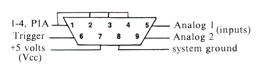
| Figure 1. Front panel pin diagram. | |
|
The Basics
As you can see from the pin diagram in Figure 1, each joystick port has several potential input sources available. For example, two of the pins are intended for use with the paddle controllers. These are called the Analog pins. They take an analog source such as a variable resistance and convert it into a digital signal. This is in essence how the paddles function. They provide a resistance via a potentiometer within the paddle unit, between the analog input pins and +5 volts DC. The computer interprets the variable voltage as a digital number between 0 and 228. This is called "on board" analog to digital conversion. Units performing a similar function may be purchased at a hefty price, but Atari owners have the use of 8 of these units built right in!
For now, let's concentrate on pins 1-4 on the joystick ports. These are the pins of the Peripheral Interface Adapter chip, more commonly referred to as the PIA. Basically the PIA provides a means of connecting your computer to peripherals. The PIA chip can be programmed for either input or output. There are two PIA ports of eight bits each available for your use. Joystick ports 1 and 2 compose PIA port A, while joystick ports 3 and 4 compose PIA port B. Each port is one byte (8 bits) and may be used together or individually to provide input and output functions. Some of these functions may be used to drive a printer or other accessory, or even a series of power relays which can control alarms, lights, appliances, motors or other device.
The snag involved in controlling larger interface devices is basically a problem of taking a small amount of power and amplifying it. The ports on your computer are not made to power anything more than another chip. The manual recommends a maximum of 1 TTL load (about 1 chip) at 50 ma tops. To be of any real use, we must be able to power at least 12 to 24 volts. This higher voltage can drive a wide variety of relays and interfaces.
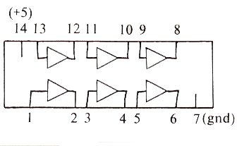
| Figure 2. SN 7407 diagram | |
|
There are several ways to accomplish this task. The most common arrangement is the transistor driver. In this arrangement the computer provides a very small voltage which turns on the transistors which in turn switch the load. A second way is through the use of opto-isolators. The computer provides 5 volts which switches the LED (light emitting diode) of the isolator. When the diode is lit, this triggers a photo sensitive transistor which is connected to a larger load or a relay.
A third way, and the one we shall use, is to employ an integrated circuit interface chip. The chip we will be using is the SN7407 made by Texas Instruments. The 7407 allows a switching of up to 30 volts from the 5 volt TTL level of the Atari, with enough current to handle a small relay. Using this one chip, we can drive up to six relays from the Atari front ports.
The SN7407, as shown in Figure 2, is an open collector device. To use it properly you must connect a 2.2K ohm resistor from each output to +5 volts. This is called a "pull up" resistor. When an output of the 7407 is "on" it is actually open so the resistor supplies power to the device you are driving. You can drive up to 30 volts at the outputs (but you may have to tamper with the value of the resistor somewhat). When an output is "off", it is shorted to ground, and your device sees 0 volts (ground actually). The resistor limits this current to a fairly low value so you don't blow the power supply or worse, the chip! Now this is the sequence of events:
Atari: HIGH (logic 1)
7407: OFF --device is OFF.
Atari: LOW (logic 0)
7407: ON --device is ON.
Since the resistor can't supply much current, the resistor/7407 combination is seen as the "ground side" of the circuit. That is, to drive a relay, we connect power to one side of the relay, and the other side to the output of the 7407. Then when we turn the relay on, Current will flow through the relay, and then through the 7407 to ground.
You can easily drive LED's this way too (such as for test lights), as well as a variety of small relays or solid state switches. Just make sure you SINK the current--that is, one end of your driven device goes to +5 (through a resistor!) and the other end to the 7407. Sending a "0" (logic level low) to the PIA turns the device ON, and a "1" (logic level high) turns it OFF. If you want to do it the other way around, use the inverting 7406 chip, which will turn your device ON with a high logic level and OFF with a low level. Recognize that the default state of the PIA when the computer is powered up is all bits high. If you are using an inverting 7406, your devices would come alive when you powered on the Atari. This is why I prefer to use the 7407, since I can power up and then have my software drive the devices by writing a 0 to the bit I want to power a device from.
Speaking of bits, a few words are in order about the structure of the ports before you run off to warm up your soldering irons. The PIA as I mentioned earlier consists of two ports, port A and port B (or PORTA and PORTB for all you mnemonic freaks). These are controlled through the use of the control registers for each port, PACTL and PBCTL. You may have heard of the PACTL because that's the one you POKE to turn on the cassette player. The addresses are as follows:
PORTA 54016/$D300 --
port A address
PORTB 54017/$D301 --
port B address
PACTL 54018/$D302 --
port A control
PBCLT 54019/$D303 --
port B control
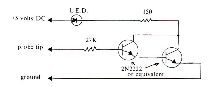
| Figure 3. Logic Probe Schematic. | |||||||
|
|||||||
On power up, the ports are initialized to $FFFF or all bits high. To use a port for input, just pull the bit of your choice low by connecting it to ground. To use the port for output, it first must be formatted for output. The procedure is not complex:
1. POKE the control register (PACTL or PBCTL) with 56/$38 hex.
2. Now poke the port (PORTA or PORTB) with 255/$FF hex. This specifies the port will be used for output.
3. Poke PACTL or PBCTL with 60/$3C hex.
4. Now just poke the port (PORTA or PORTB) with your data.
Essentially you have a total of 16 bits to play with. Just remember that two joystick ports make up one PIA port. Stick 0 and 1 are the A side and stick 2 and 3 are side B. Each joystick port is 4 bits or 1 nibble. Each side of the PIA is 8 bits or 1 byte. When programming for output, you must remember that a specific BIT is driving a device. Therefore one joystick port can drive 4 devices (1 for each bit). An entire PIA side will handle 8 devices and if you use both A and B sides you can trigger 16 individual devices at once or in any combination. You must POKE into that port a decimal number whose BINARY representation will switch on a certain bit or series of bits. For example, if I POKE a 255 into port A, all bits would be on. If I POKE a 12 into port A, bits 3 and 4 only would be on, since the binary of 12 is 1100 The individual joystick ports may be read using the shadow registers as follows:
Jack 1 (STICK 0) 632/$278 hex
Jack 2 (STICK 1) 633/$279 hex
Jack 3 (STICK 2) 634/$27A hex
Jack 4 (STICK 3) 635/$27B hex
Each port will return a number between 0 and 15. You also can use the BASIC keywords STICK to access these ports eg. X=STICK(0), etc.
The Hardware Part
Generally, all of the circuits we will describe can be breadboarded in any way convenient for you. For those of you just starting out, and who want to do some experimenting, I recommend the following workbench supplies:
-- a solderless breadboard or wirewrapping set-up for prototyping your circuitry. (Such as those made by Vector, Tandy, etc.)
-- a variety of IC and transistor sockets
-- an anti-static mat or spray
In addition, for this project, you will need at least one DE9S connector to match the front joystick port, and some multi-conductor wire.
Now let's get started by building another useful tool for you to use: a logic probe. Figure three shows the construction diagram of a two-transistor logic probe. You can "steal" the necessary 5 volts from the computer on board power supply. When the LED is on this indicates a logic 1 or high condition. No LED indicates a 0 or low. (Actually that is not exactly true. This logic probe cannot detect the actual "0" state. There are more sophisticated probes able to differentiate high, low, and high impedance logic states but what do you want for less than a buck?)
One potential way to mount the probe is to build the unit on a small (1" by 2") perfboard, and then slide the completed assembly into a large cigar tube. A small probe tip could then be soldered to the front of the cigar tube, and wires for the required 5 volts and ground could come out the back end. These would terminate in small alligator clips.
| Figure 4. 7407 Interface (1 gate). | |
|
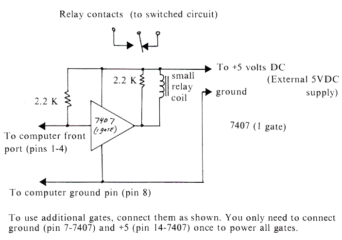
To use additional gates, connect them as shown. You only need to connect ground (pin 7-7407) and +5 (pin 14-7407) once to power all gates.
A Useful Interface Board
Figure four is a schematic diagram of an output interface board which is connected to the front ports of the computer.
The heart of the circuit is the 7407 chip. As you can see, the input channels of the 7407 are connected to the front port by way of the 2.2K pullup resistor. Even though the port initializes to FFFF (or all ones), this maintains a high state until we do otherwise.
The output of the 7407 provides the ground side of a relay circuit. The relay coil is connected to the 5 volt supply (NOT the one on the computer port!). When the 7407 is activated by having one of the front port pins pulled low, it provides the relay coil with a path to ground, and the coil energizes. The relay controlled by the coil can be used to switch on just about anything, including other relays to drive larger loads.
During construction be careful that all the pins of the 7407 and the components are wired correctly. Do not forget the pull-up resistors or the small capacitors. These help prevent power supply interference. If you wish, you can substitute small LED's or 5 volt pilot lamps for the relays. This will allow you to see the ports in action.
Be sure to use an external power supply or 5 volt source. The ground of your source should be connected to the ground pin on the computer. You will not need the 5 volt pin. Incidentally, you can use the external supply to power your logic probe, and still read the computer logic signals at the ports.
Now For a Little Software
The program listing will provide you with a demonstration on how the ports are programmed. The program first allows you to select a port, and program it for either input or output. Then you can write data to the port and the computer will peek the port and verify the data you wrote. You can also do this by using the logic probe. You will get a logic 1 for every active bit in the port.
10 REM * PROGRAM TO FORMAT PIA PORTS
20 REM
30 GRAPHICS 0:POSITION 10,2
40 DIM IO$(10),DATA$(3)
50 PRINT "PIA PORT DEMO"
60 REM
70 REM PORT ADDRESS
80 REM
90 PORTA=54016:PORTB=54017
100 REM
110 REM * ROUTINE TO CONFIGURE PORT
120 REM
130 TRAP 130:PRINT :PRINT "Configure which port (1-4) ";
140 INPUT PORT:IF PORT<1 OR PORT>4 THEN 130
150 REM
160 REM SELECT PORT CONTROL REGISTER
170 REM ADDRESS (PACTL,PBCTL)
180 REM
190 IF PORT<3 THEN PCTL=54018:PORT=PORTA
200 IF PORT>2 THEN PCTL=54019:PORT=PORTB
210 PRINT :PRINT
220 REM
230 REM SELECT INPUT OR OUTPUT
240 REM
250 PRINT "Input or Output ";
260 TRAP 250:INPUT IO$
270 IF IO$(1,1)="I" THEN F=0:GOTO 340
280 IF IO$(1,1)="O" THEN F=255:GOTO 340
290 GOTO 250
300 PRINT
310 REM
320 REM CONFIGURE THE PORT
330 REM
340 POKE PCTL,56
350 POKE PORT,F
360 POKE PCTL,60
370 PRINT :PRINT
380 REM
390 REM ENTER YOUR DATA
400 REM
410 IF IO$(1,1)="I" THEN PRINT "PORT  IS  FORMATTED  FOR INPUT":PRINT :GOTO 130
420 PRINT "NOW ENTER YOUR DATA"
430 PRINT "(ENTER A RETURN TO DO ANOTHER PORT)"
440 INPUT DATA$:IF DATA$="" THEN PRINT CHR$(125):GOTO 130
450 TRAP 530
460 REM
470 REM POKE DATA TO PORT/VERIFY IT
480 REM
490 POKE PORT,VAL(DATA$)
500 PRINT "VERIFY ";PEEK(PORT)
510 GOTO 440
520 END
530 TRAP 40000:PRINT "INPUT ERROR, RE-ENTER ";:GOTO 440
Marshall S. Dubin, 2639 Hempstead, Auburn Heights, Michigan 48057.
Table of Contents
Previous Section: Neater Numerical Tables
Next Section: Atari Strings and Text Handling